

West Chester University

Something happens when you find yourself here. You find your passion. You find it in labs, lectures, out in left field. You find it on stage, behind a camera, in front of a blank page. You find more than a direction. You find your element.
Find Your Program
Choosing a program begins a transformative journey. Here you will find a range of options—some science learning, majors for creative types, and several somewhere in between—and whatever direction you choose, you will find a path to a wiser you.


Find Your Element. Feed your mind.Academics
With over 180 diverse academic opportunities, West Chester University has made it possible for every student to find their element. With degrees ranging from accounting to African American studies to marine biology, we’re confident that our students can find what they love and make it their own.
So Much Life. So Many Things.Student Life
Everyone has their thing, and no matter what yours happens to be, we're confident you can find it among our 300+ clubs and organizations. Whether you’re interested in the NAACP or the Bollywood dance club, passion is in our DNA and it is our priority that we help you find yours.


Let the Journey Begin.Admissions
When you choose WCU you choose discovery. With 64 undergraduate programs, 43 tracks, 90 minors and 44 fields of study—not to mention the close proximity to Philly, DC and NYC—you can't avoid finding new perspectives, new passions, a new you.
Where
you least
expect
it, you'll
find it.

When the
reaction
surprises
you, you'll
find it.

When
you are
here,
you'll find
it.
Demand for a West Chester University education remains high and consistent growth continues with more than 16,500+ undergraduate and graduate students. A constant forward motion propels this distinctive University; it is fueled by our relentless resolve to help students be successful.
- West Chester University President Chris Fiorentino, Ph.D.
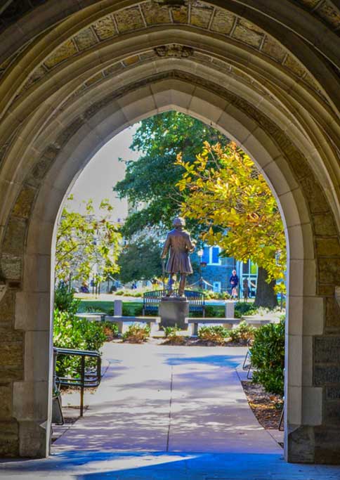
Location
We're proud of our beautiful campus and the unique charm that defines West Chester. But with three of the country's most dynamic cities - DC, Philadelphia and New York City - just a short ride away, escapes are kind of necessary.
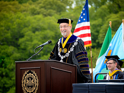
West Chester University to Honor
President Christopher M. Fiorentino
on April 26 at 12 p.m.
West Chester University News


Media Guide
to WCU Faculty Experts
Visit the Media Guide to WCU Faculty Experts to find a faculty member with expertise in a specific field.


Upcoming Events

president fiorentino retirement celebration
Friday, April 26, 2024, 12 - 2pm
mather planetarium show
Friday, April 26, 2024, 7 - 8pm
university dance company’s annual spring dance concert
Saturday, April 27, 2024, 2 - 3pm
wcu wind ensemble concert
Sunday, April 28, 2024, 3 - 4:30pm
